Dr. Abdul Kaium Mia
About me!
I am a researcher with a focus on 2D materials (TMDs) for optoelectronics devices. I have completed my PhD from the Centre for Nanotechnology, IIT Guwahati, and am looking for postdoc positions.
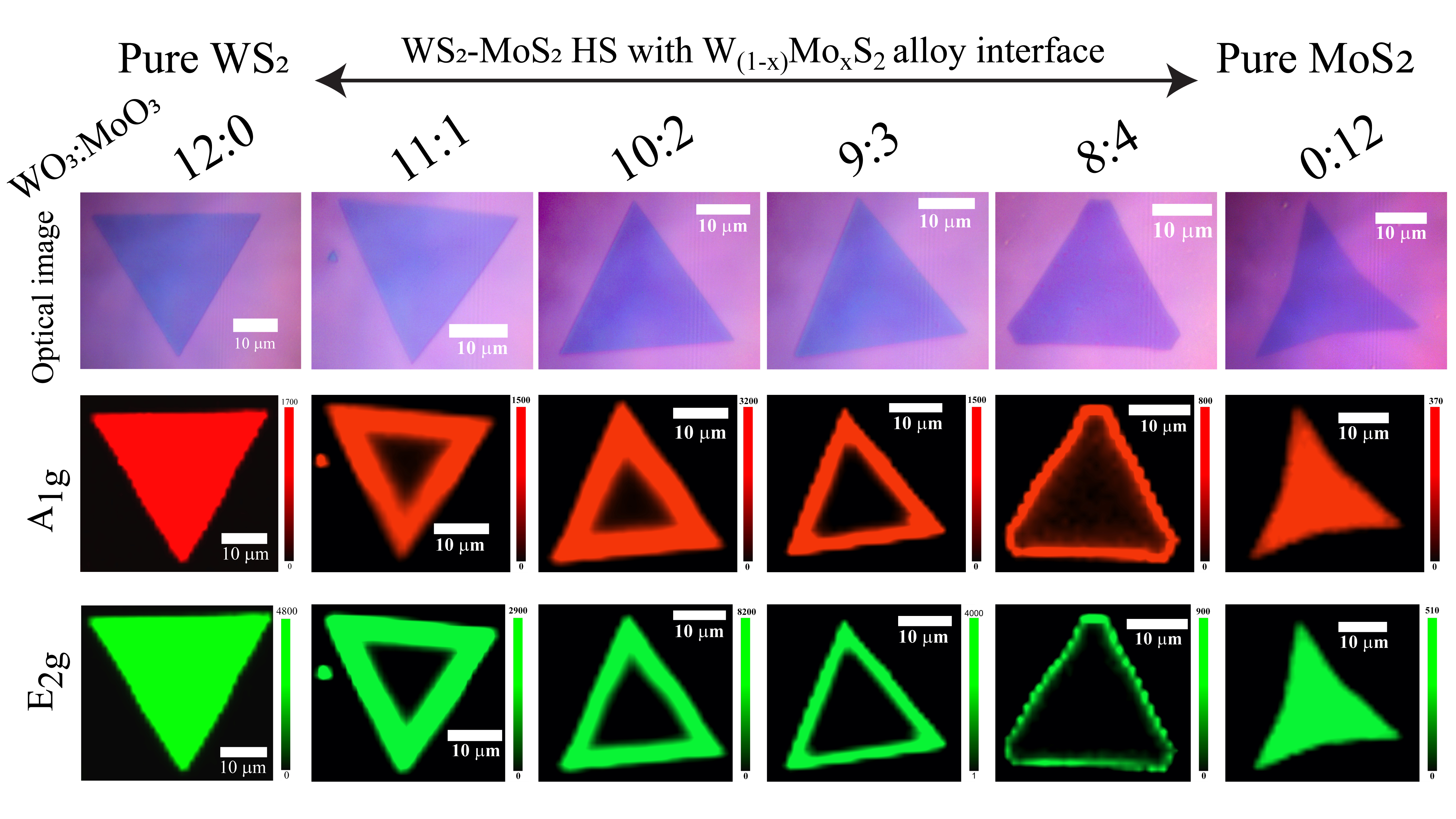
During my PhD I have studied the layer-controlled CVD growth of WS₂, MoS₂, and WS₂-MoS₂ in-situ lateral heterostructures with an alloy interface using chemical vapor deposition (CVD) techniques, alongside their applications in broadband photodetection, high-performance field-effect transistors (FETs), flexible electronics, and biosensing.
My notable contribution during my PhD includes single-step in-situ growth of WS₂-MoS₂ heterostructure for high performance optoelectronics and asymmetric contact induced selective doping in bilayer WS₂ for enhanced photodetection, which has been listed in Spotlight on Materials and Nano Research from Indian institutes and Nanoscale Most Popular 2024 Articles.
Recent Publications
Click any image below to view the corresponding manuscript:
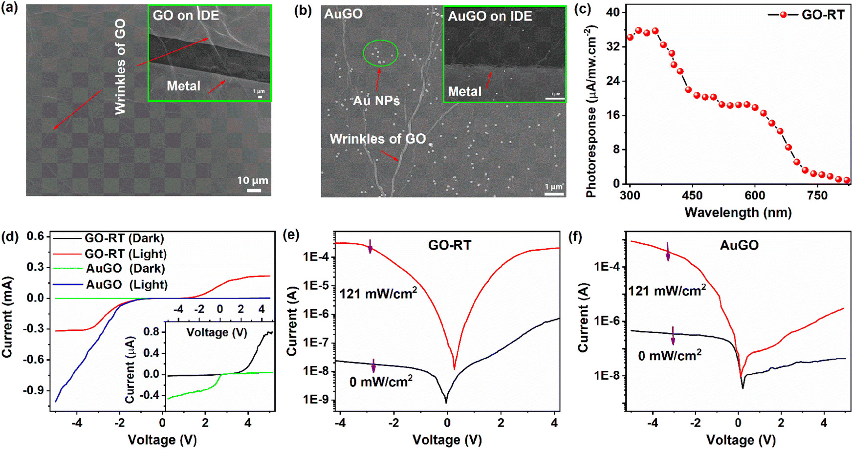
The molayer MoS₂ based flexible Photodetector(Journal of Materials Chemistry C , 2025)
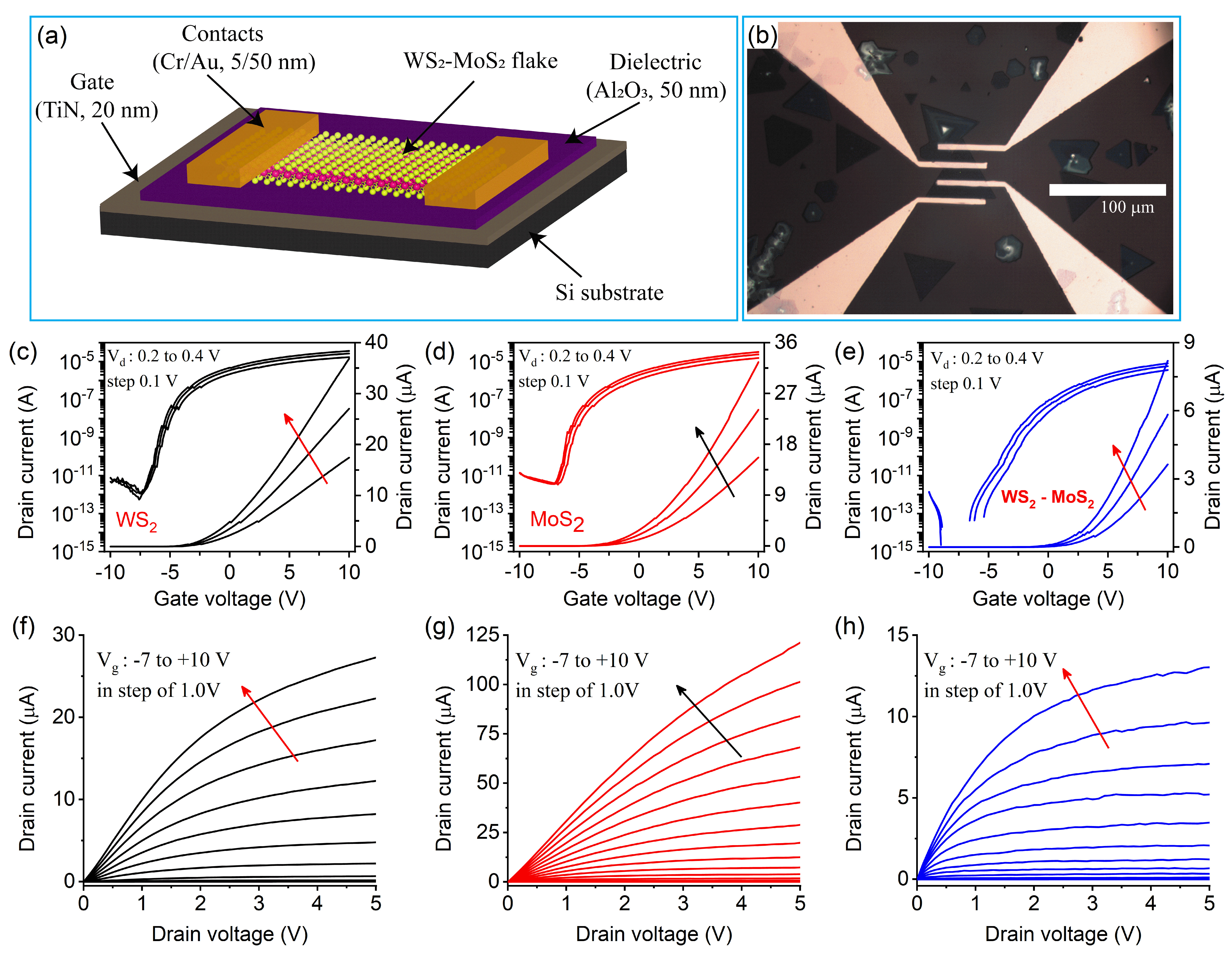
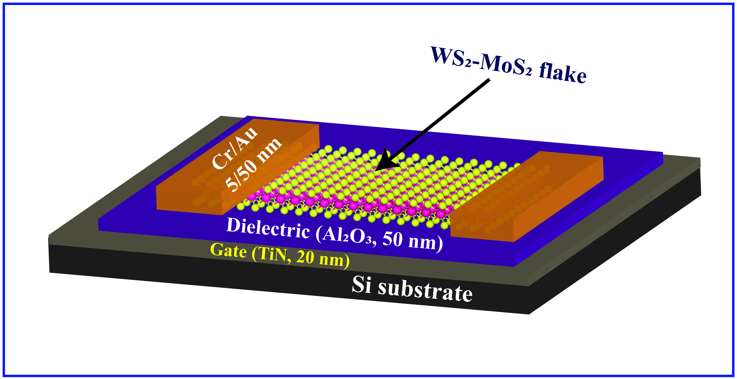
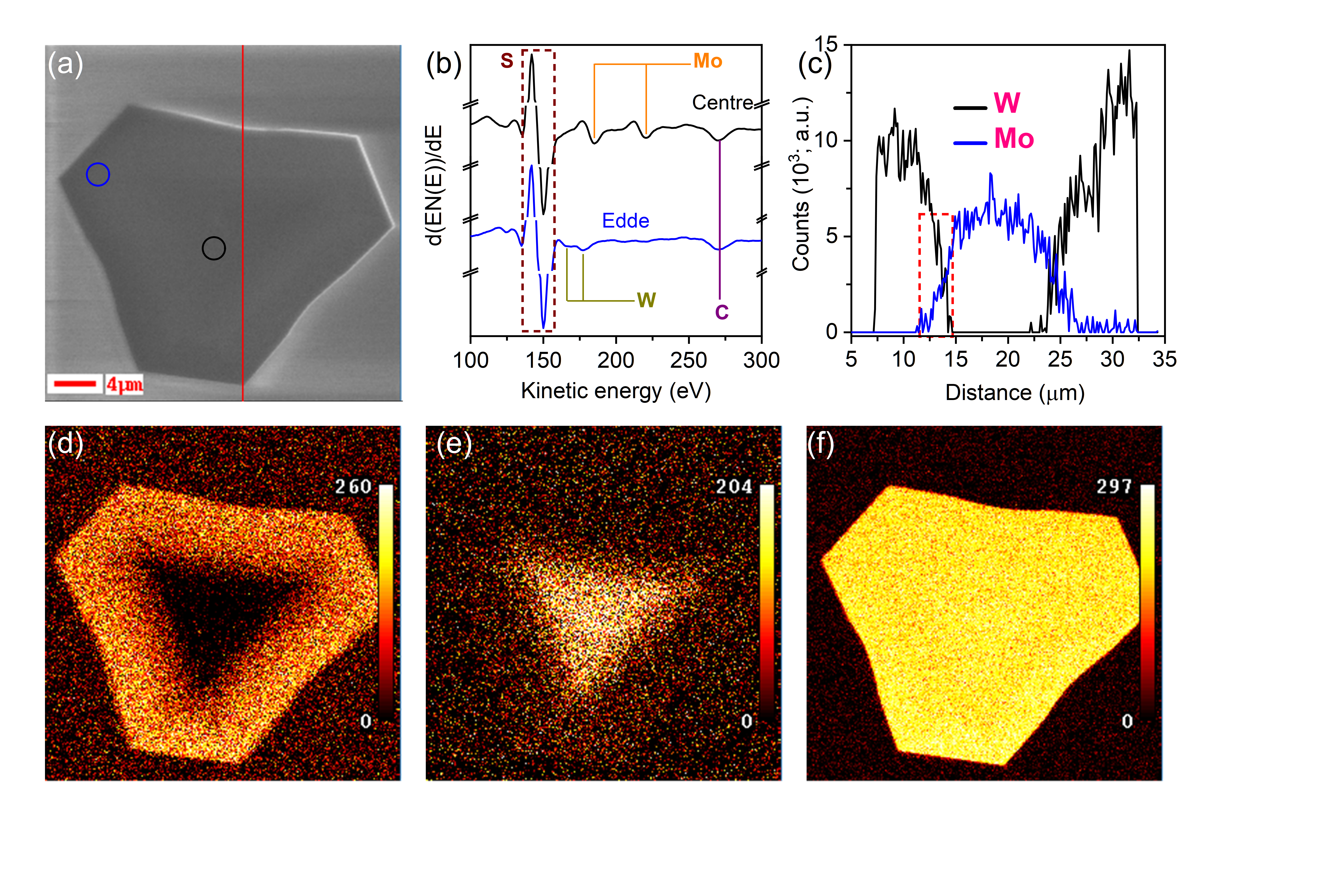
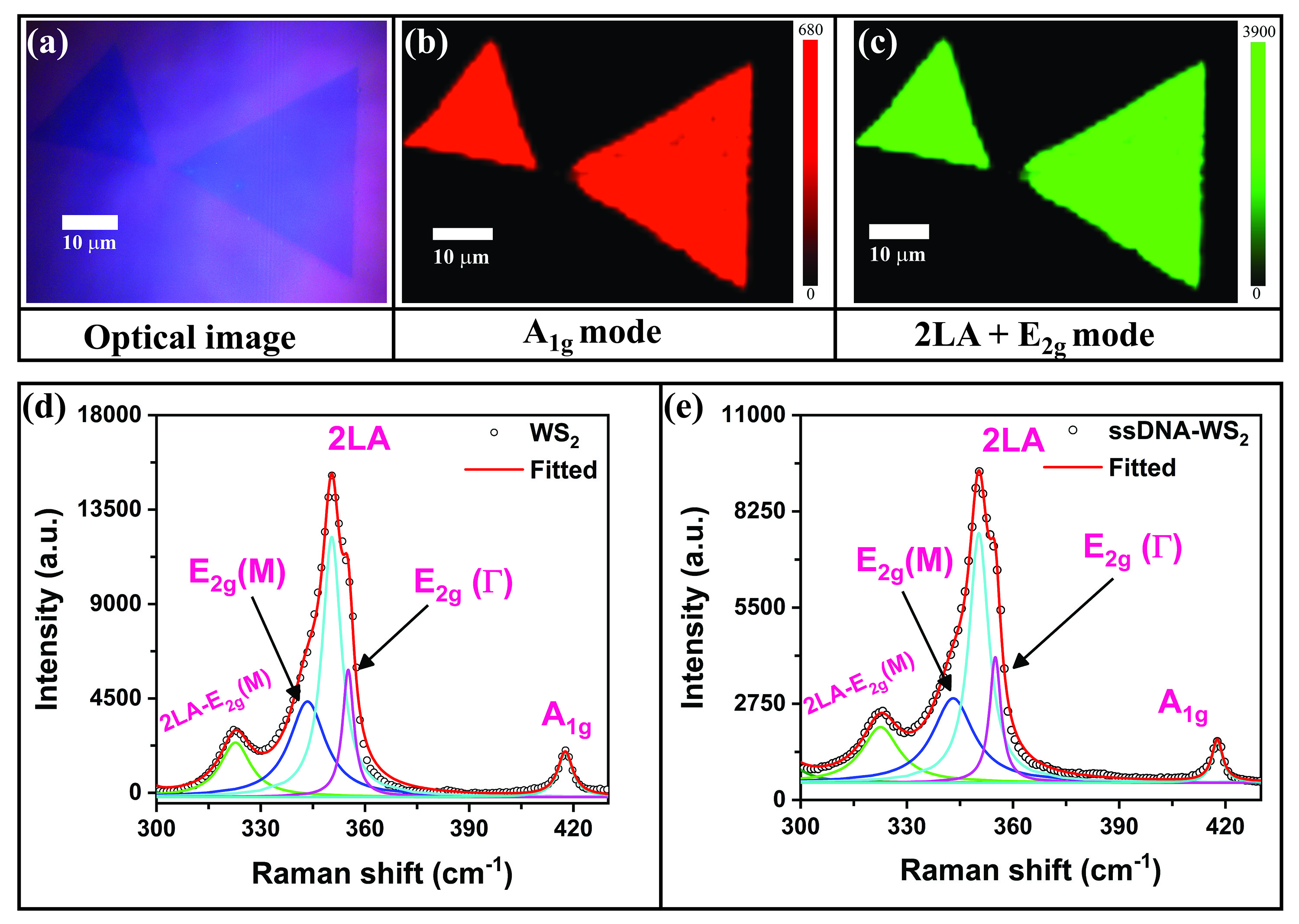
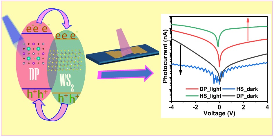
WS₂–MoS₂ Lateral Heterostructure (Materials Today Nano, 2025)
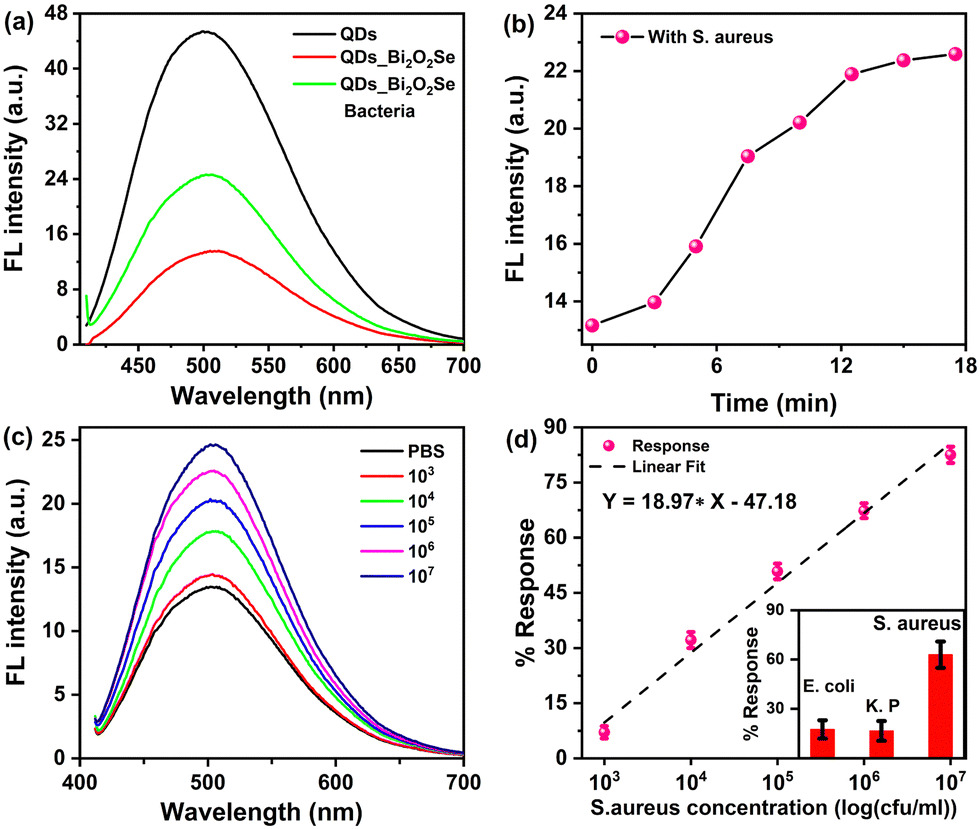
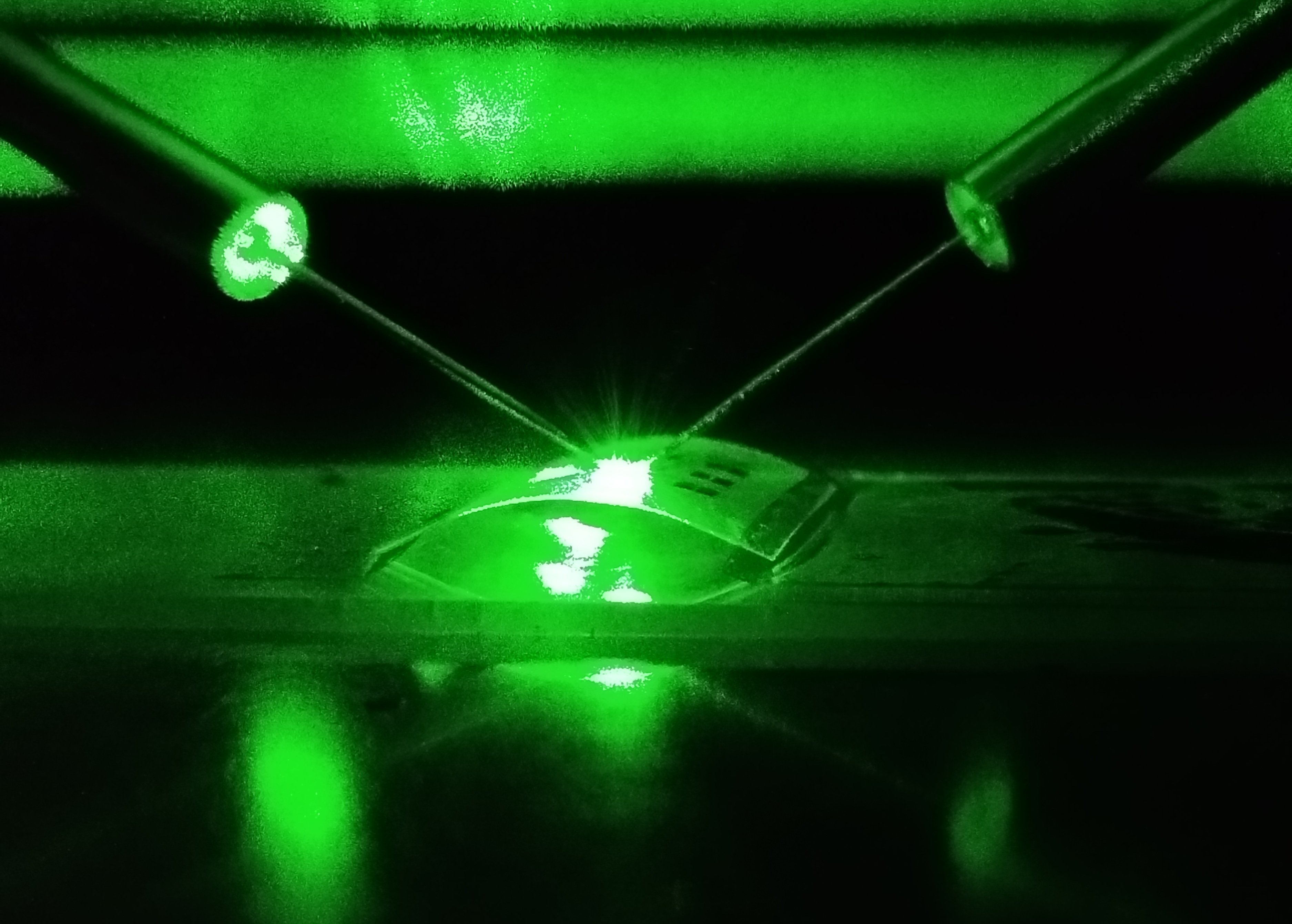
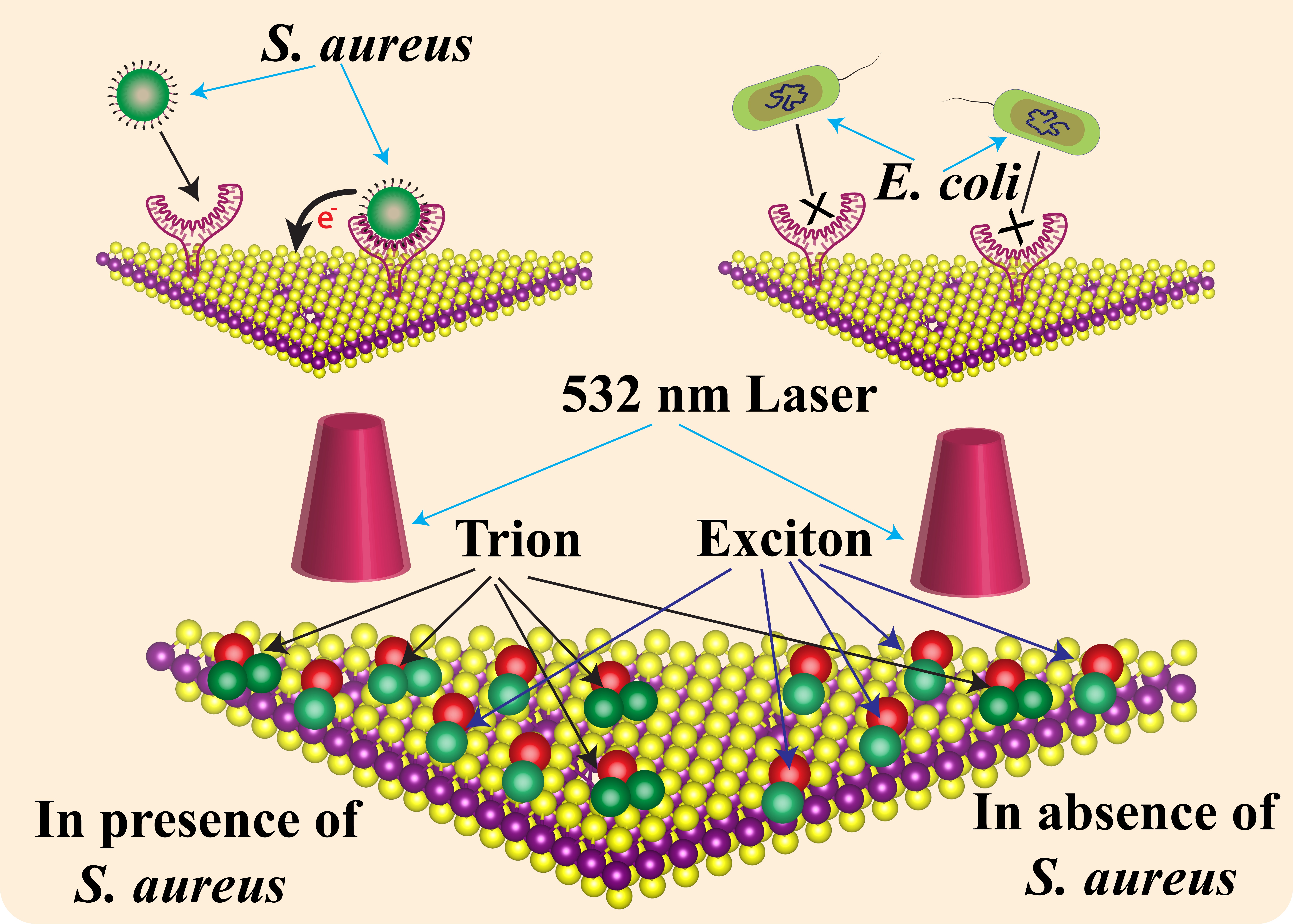
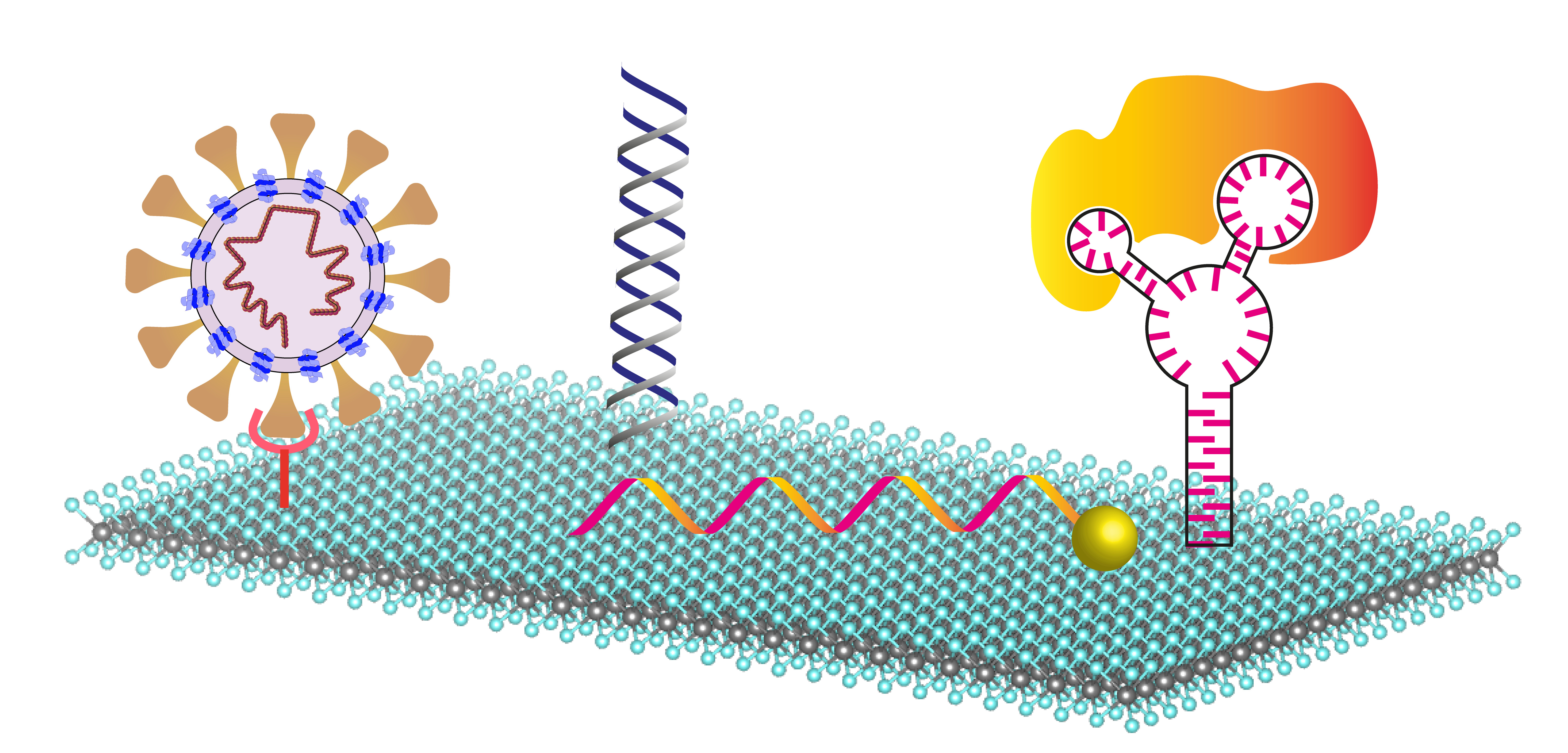
Fast detection of S. Aureus (Journal of Materials Chemistry B, 2024)
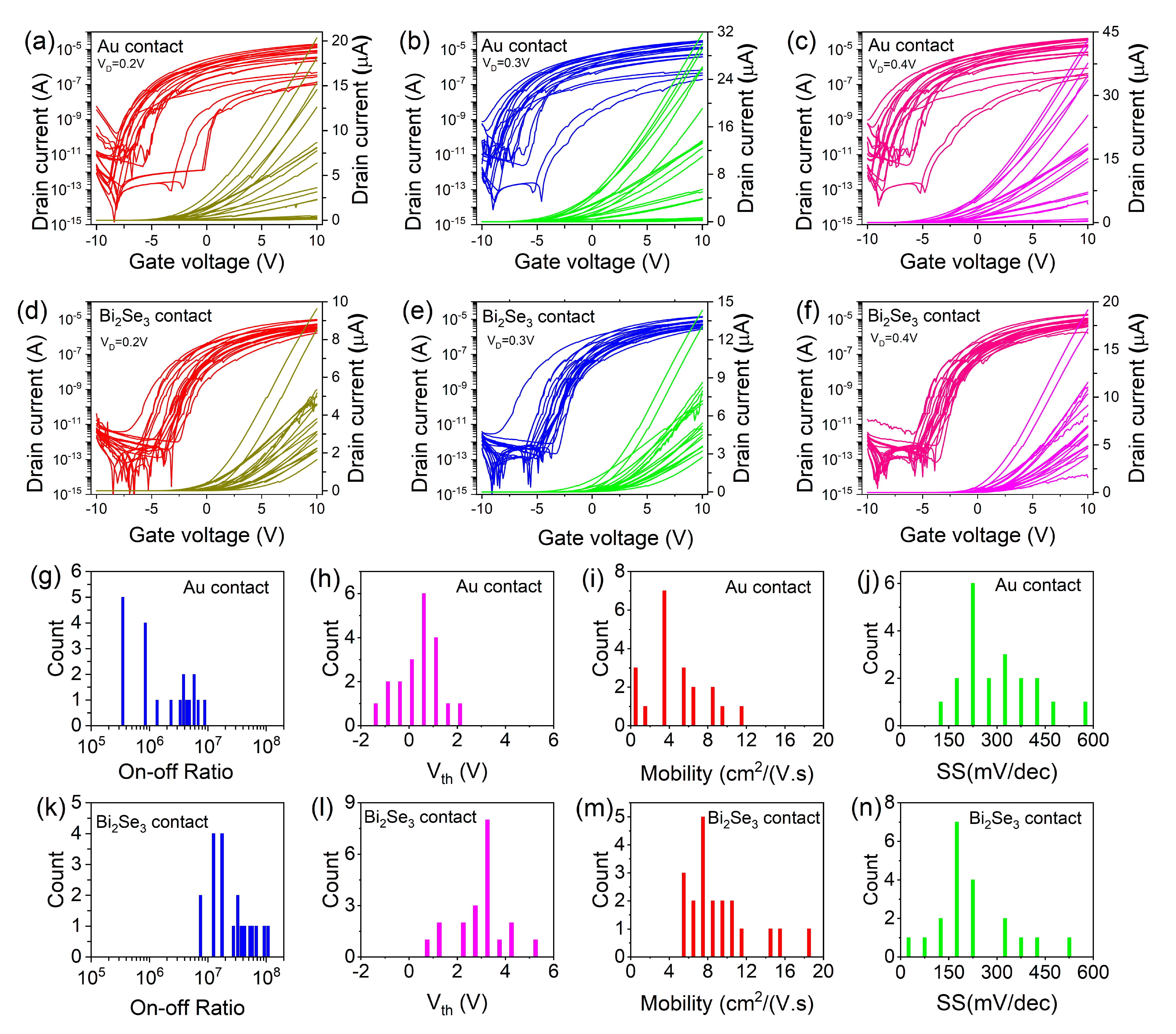
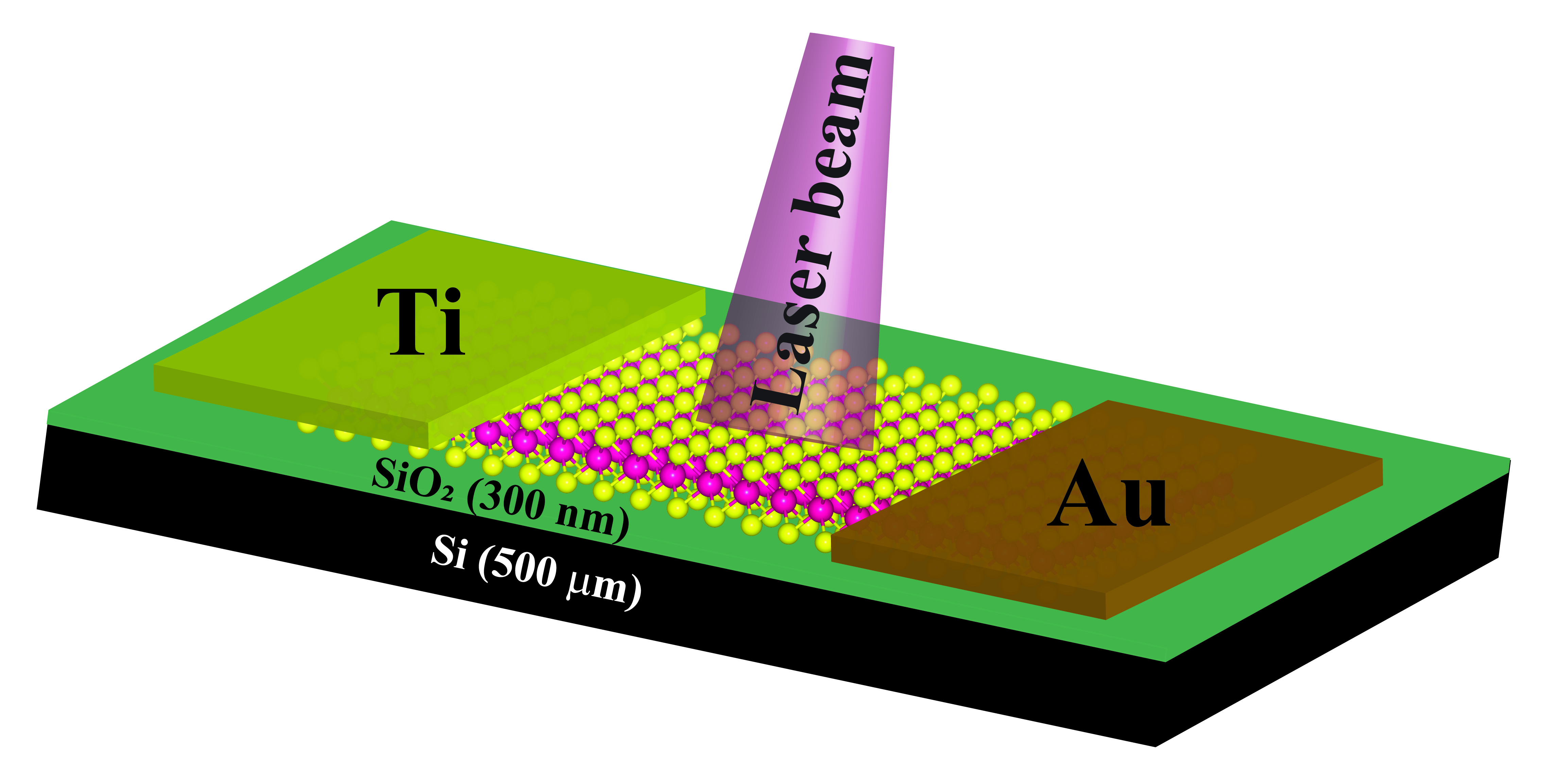
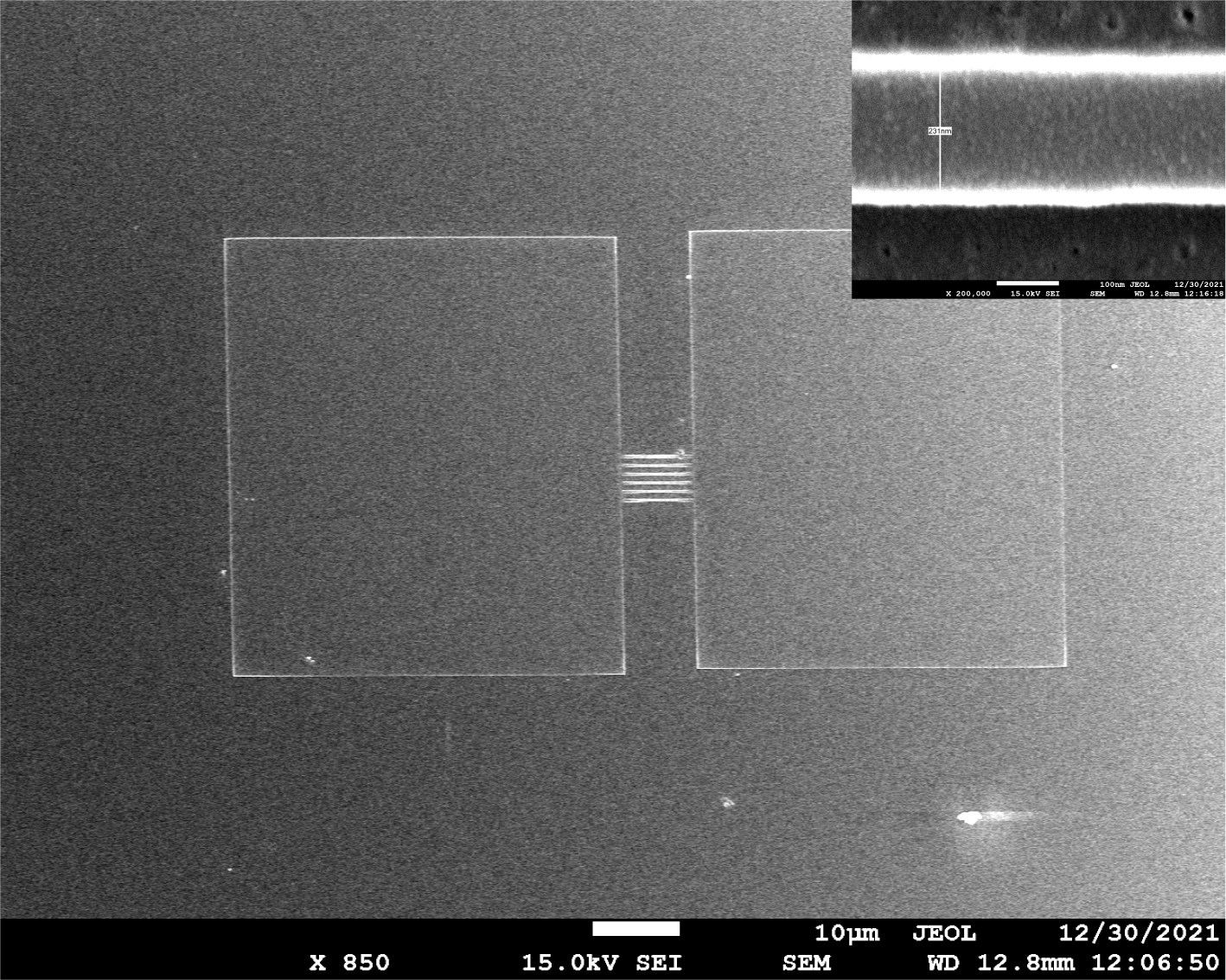
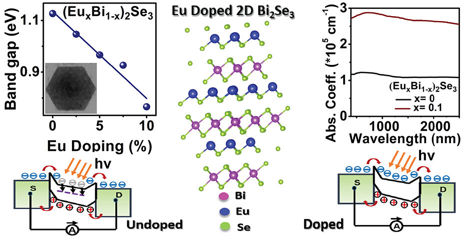
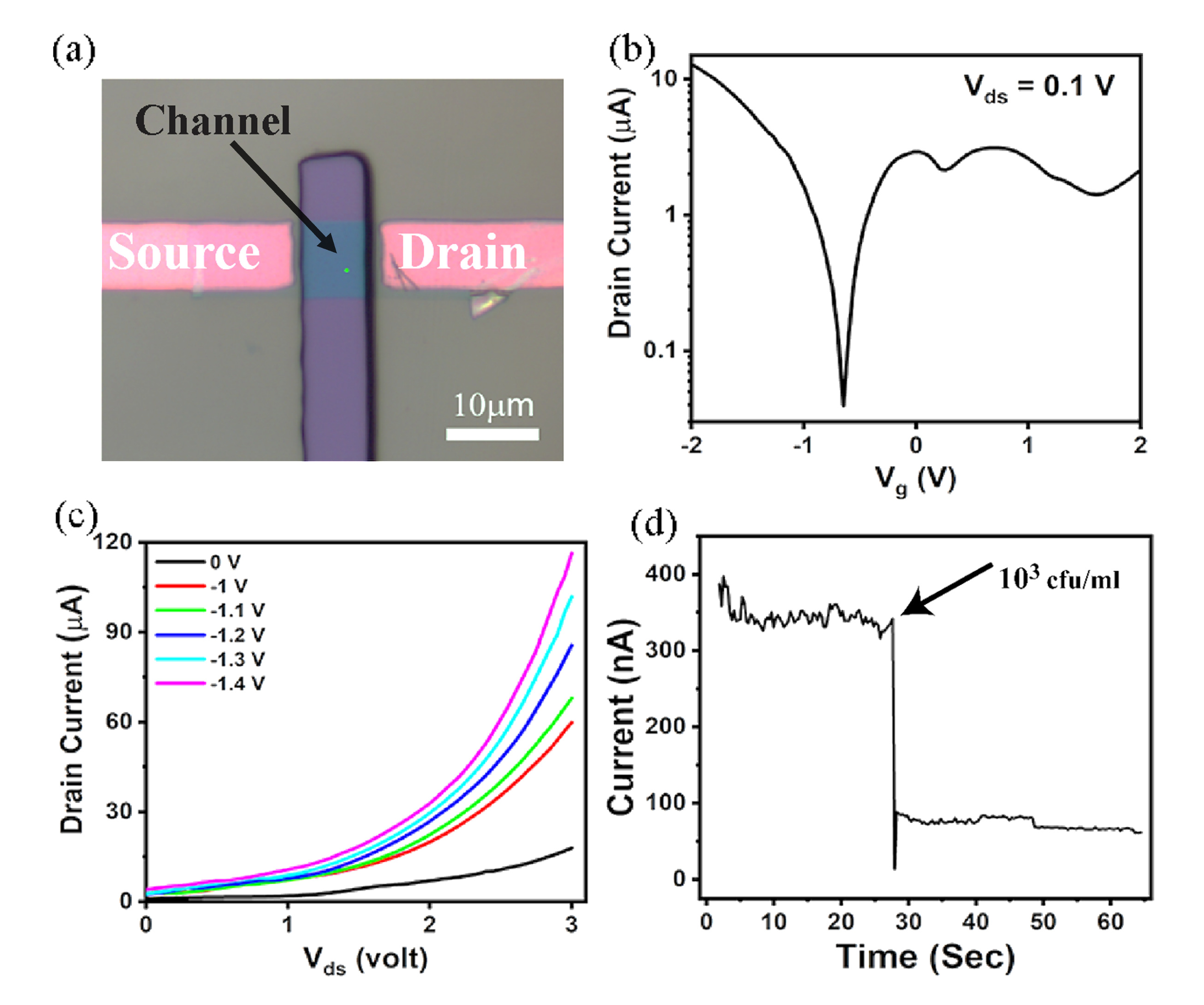
Asymmetric contact-based bilayer WS₂ Photodetector (Nanoscale, 2024)
S. Aureus detection using Aptamer functionalized monolayer WS₂ (Sensors and Actuators Reports, 2024)
Manipulating Trion and Biexciton Emissions in Monolayer WS₂ (ACS Applied Nano Materials, 2024)
Education
Experience
Contact Information
Location
Advanced Nanomaterials and Nanosensors Lab
Centre for Nanotechnology
Indian Institute of Technology Guwahati
Guwahati, Assam 781039, India
Research Interests
- CVD growth of 2D semiconducting materials and heterostructures
- Carrier dynamics and charge transport in 2D semiconductors
- Spectroscopic & microscopic analysis of 2D materials
- Optoelectronic applications: Photodetectors, FETs, Biosensors
Research Areas
CVD Growth of 2D Materials
FET Devices
Photodetector Applications
2D Heterostructures
Spectroscopic Analysis
Flexible Devices
Advanced Lithograpgy
Biosensing Technology
Research Methodology
My research employs a series of experimental techniques to explore the fundamental properties and applications of CVD-grown 2D materials:
- Chemical Vapor Deposition (CVD) for material synthesis
- Raman spectroscopy and photoluminescence for characterization
- Atomic force microscopy and transmission electron microscopy
- Device fabrication and electrical measurements
List of Publications
Conferences & Workshops
- Recent Progress in Graphene and 2D Materials Research (RPGR-2023), Bangalore, India.
- 5th International Conference on Nanoscience and Nanotechnology (ICONN-2019), SRM IST, India.
- 8th International Conference on Advanced Nanomaterials and Nanotechnology (ICANN), IIT Guwahati, India.
- Frontiers in Nano-Sciences 2024 (FINS 2024). IIT Guwahati, India.
- International Symposium on Semiconductor Materials and Devices (ISSMD-2022), KIT, India.
- International Conference on Nano-Structured Materials & Devices (ICNSMD-2018), University of Delhi, India.
- Advances in Catalysis for Energy and Environment (CACEE-2018), TIFR, India.
- Hands-on Training Workshop on Nanofabrication Technologies, IISc Bangalore, India.
- XXI International Workshop on Physics of Semiconductor Devices (IWPSD 2021), IIT Delhi, India.
- SPARC Workshop on 2D Materials, 2024.